1. Designed growth of large bilayer graphene with arbitrary twist angles
北京大学刘开辉,上海科技大学王竹君等,Nature Materials,21 1263-1268(2022)
doi.org/10.1038/s41563-022-01361-8
The production of large-area twisted bilayer graphene (TBG) with controllable angles is a prerequisite for proceeding with its massive applications. However, most of the prevailing strategies to fabricate twisted bilayers face great challenges, where the transfer methods are easily stuck by interfacial contamination, and direct growth methods lack the flexibility in twist-angle design. Here we develop an effective strategy to grow centimetre-scale TBG with arbitrary twist angles (accuracy, <1.0°). The success in accurate angle control is realized by an angle replication from two prerotated single-crystal Cu(111) foils to form a Cu/TBG/Cu sandwich structure, from which the TBG can be isolated by a custom-developed equipotential surface etching process. The accuracy and consistency of the twist angles are unambiguously illustrated by comprehensive characterization techniques, namely, optical spectroscopy, electron microscopy, photoemission spectroscopy and photocurrent spectroscopy. Our work opens an accessible avenue for the designed growth of large-scale two-dimensional twisted bilayers and thus lays the material foundation for the future applications of twistronics at the integration level.
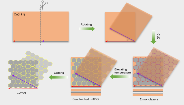
Fig.1 A piece of single-crystal Cu(111) foil was cut into two pieces with parallel edges (marked in red and violet). Then, the two pieces were stacked with rotation angle α between the two marked edges. After that, graphene was epitaxially grown between the two adjacent Cu(111) surfaces by the CVD method. Bilayer graphene with twist angle α was subsequently obtained by heating the Cu to an elevated temperature and was finally isolated after etching the Cu away.
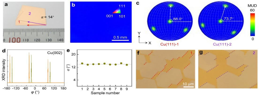
Fig.2 Photograph of two stacked Cu foils with rotation angle α. The numbers on the ruler indicate the length in millimetres. b, EBSD IPF map of the Cu foil. The uniform blue colour reveals the single-crystal structure of the (111) facet index. c, EBSD PFs of the two Cu pieces, marked as Cu(111)-1 and Cu(111)-2. The multiples of uniform density (MUD) results present a relative rotation angle of 14.3°. d, XRD φ-scan data for Cu(111)-1 (orange curve) and Cu(111)-2 (dark yellow curve) obtained by fixing along the Cu(002) direction. The three-fold symmetry of diffraction peaks indicates the high crystallinity and a shift of 14.2° between the two spectra. e, Statistical data of the rotation angles for nine stacked Cu foils measured by EBSD, indicating the small deviation of ~1.0°. f,g, Optical images of the hexagonal graphene domains on the top surfaces of Cu(111)-1 (f) and Cu(111)-2 (g), with a relative rotation angle of ~14°.
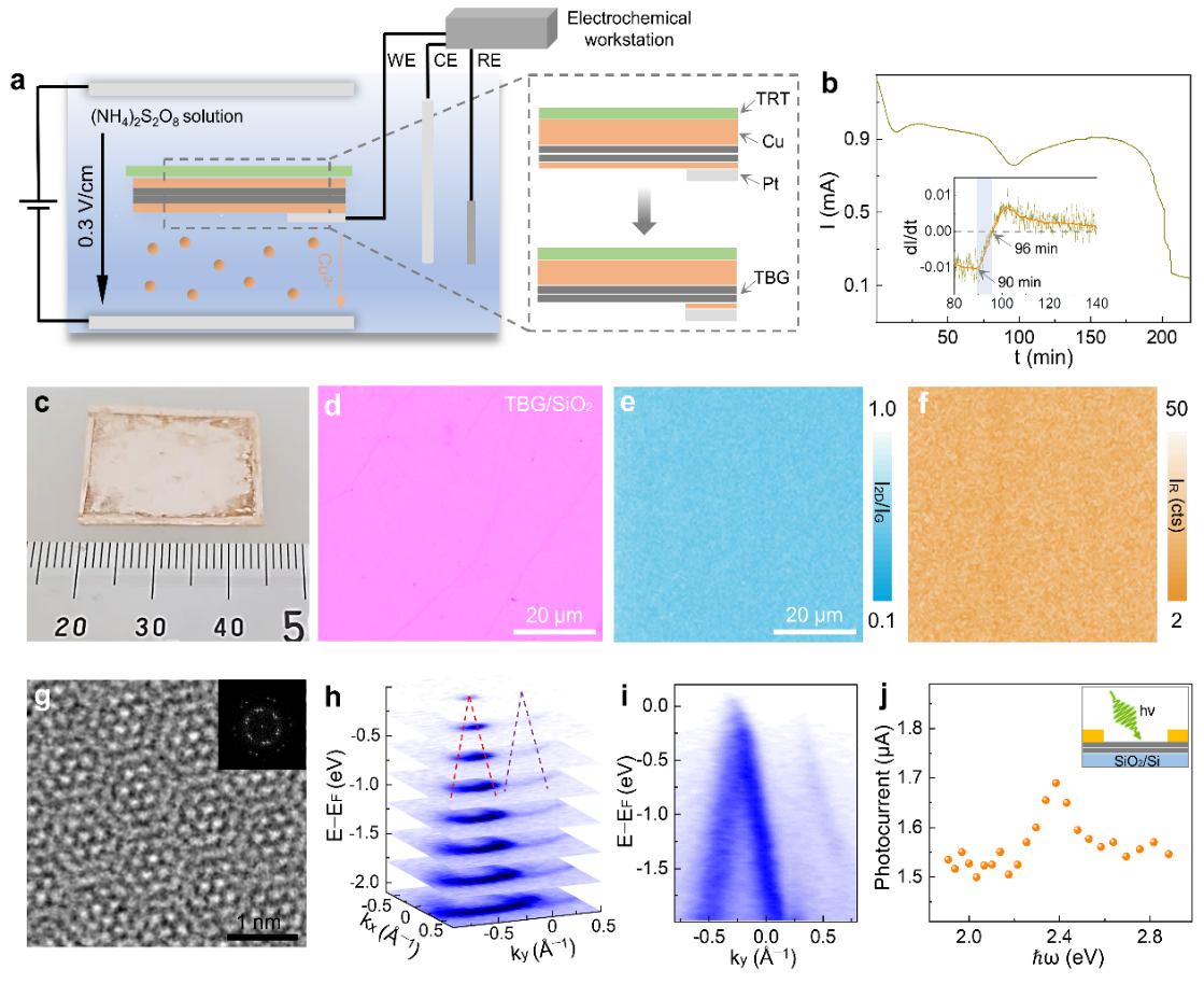
Fig.3 a, Schematic of the equipotential surface etching process. TBG was obtained by etching one side of the Cu(111) foil with the other side protected by TRT. The three-electrode system consists of a working electrode (WE), reference electrode (RE) and counter electrode (CE). b, Time (t) evolution of current (I) during the etching process. The inset shows the time evolution of the derivative of current during the etching process. c, Photograph of the Cu(111) foil with a freshly exposed bilayer graphene film. The numbers on the ruler indicate the length in millimetres. d, Optical image of bilayer graphene after transferring onto the SiO2/Si substrate. e,f, Raman mappings of I2D/IG and IR, verifying the uniformity of the obtained bilayer graphene film. g, HRTEM image of bilayer graphene. The inset shows the fast Fourier transform pattern of the HRTEM image. h, Stacking plot of constant-energy contours at different binding energies in kx–ky plane of the bilayer graphene. i, ARPES spectrum of the bilayer graphene across the two adjacent Dirac cones of h along the ky direction. j, Photocurrent versus the photon energy (ħω) of incident light. These results prove that the twist angle of bilayer graphene is ~14°.
2. Topology Hierarchy of Transition Metal Dichalcogenides Built from Quantum Spin Hall Layers
上海科技大学陈宇林,柳仲楷,清华大学何珂等
Advanced Materials, 2300227, (2023) doi.org/10.1002/adma.202300227
The evolution of the physical properties of 2D material from monolayer limit to the bulk reveals unique consequences from dimension confinement and provides a distinct tuning knob for applications. Monolayer 1T'-phase transition metal dichalcogenides (1T'-TMDs) with ubiquitous quantum spin Hall (QSH) states are ideal 2D building blocks of various 3D topological phases. However, the stacking geometry has been previously limited to the bulk 1T'-WTe2 type. Here, the novel 2M-TMDs consisting of translationally stacked 1T'-monolayers are introduced as promising material platforms with tunable inverted bandgaps and interlayer coupling. By performing advanced polarization-dependent angle-resolved photoemission spectroscopy as well as first-principles calculations on the electronic structure of 2M-TMDs, a topology hierarchy is revealed: 2M-WSe2, MoS2, and MoSe2 are weak topological insulators (WTIs), whereas 2M-WS2 is a strong topological insulator (STI). Further demonstration of topological phase transitions by tunning interlayer distance indicates that band inversion amplitude and interlayer coupling jointly determine different topological states in 2M-TMDs. It is proposed that 2M-TMDs are parent compounds of various exotic phases including topological superconductors and promise great application potentials in quantum electronics due to their flexibility in patterning with 2D materials.
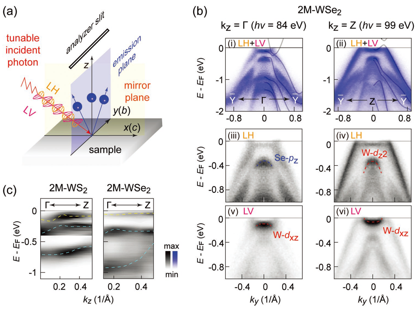
Fig.4 Photon-energy- and polarization-dependent angle-resolved photoemission spectroscopy (ARPES) measurements. a) Schematic polarization geometry used in the ARPES experiment, where the linear horizontal (LH) and linear vertical (LV)-polarized light are incident on the sample parallel and perpendicular with respect to the detection plane (xz-plane). b)(i) and (ii) Polarization-integrated ARPES results of 2M-WSe2 dispersion along (i) 𝑌¯−𝛤−𝑌¯ with a photon energy of 84 eV and (ii) 𝑌¯−𝑍−𝑌¯ with a photon energy of 99 eV. The corresponding calculation is appended. (iii)-(vi) Polarization-dependent ARPES results of 2M-WSe2 dispersion along 𝑌¯−𝛤−𝑌¯ and 𝑌¯−𝑍−𝑌¯ near EF. ARPES results are symmetrized with respect to ky = 0 based on the crystalline symmetry. Blue and red dashed lines are guides to the eyes, which indicate the bands mainly contributed by specific Se and W orbitals, respectively. See more details in Note S3 and S10 (Supporting Information). c) Photon-energy-dependent ARPES measurements on the kz dispersion of 2M-WS2 and 2M-WSe2. The yellow and cyan dashed lines representing the three topmost valence bands are guides to the eyes.
Nano-ARPES测试结果及细节
附件下载: